SHANNON, CLARE, IRELAND, September 14, 2026 /EINPresswire.com/ — Announcing a new publication from Opto-Electronic Sciences; DOI 10.29026/oes.2026.260021
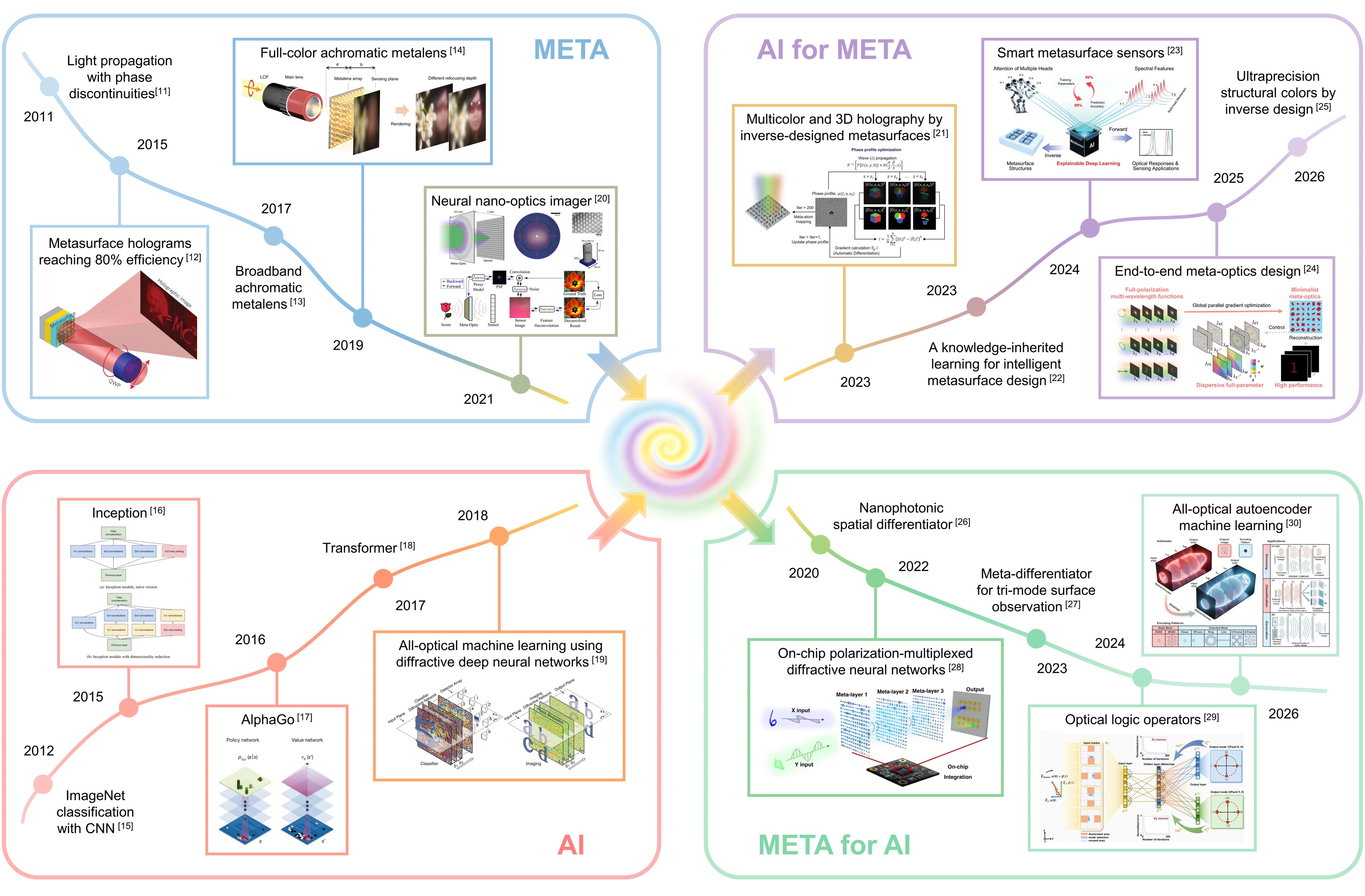
This article reviews the mutual empowerment between artificial intelligence and metasurfaces, characterizing that artificial intelligence enables intelligent nanophotonics, while metasurfaces facilitate optical intelligence. Key advances, practical applications, and future directions along these two bidirectionally evolving pathways are systematically surveyed, covering physical modeling and structural optimization, as well as optical mathematical computing and optical neural networks, providing significant insights toward chip-scale, self-adaptive, and highly intelligent photonic systems.
Artificial intelligence has transformed how information is acquired, processed and utilized, with visual information playing a vital role in perception and decision-making. The explosive growth in the volume and complexity of visual data imposes stringent requirements on optical systems with higher density, greater precision, and lower consumption. Conventional optical components, typically bulky and functionally fixed, are inadequate for dynamic environments. Meanwhile, the continuous scaling of intelligent algorithms poses challenges in computational efficiency, hardware portability and real-time response. These challenges call for a new generation of optical hardware featuring ultracompact footprints, ultrafast operation, multifunctionality and high tunability.
Metasurfaces, planar arrays of subwavelength artificial nanostructures capable of precisely tailoring the amplitude, phase, and polarization of light, have emerged as promising platforms for optical information processing, offering significant advantages in multifunctionality, parallelism, and integration density. Meanwhile, advances in artificial intelligence algorithms, such as Transformer architectures, diffusion models, and generative frameworks, have provided powerful tools for reshaping the simulations and optimizations of optical elements. Thus, metasurfaces and artificial intelligence have evolved along largely independent yet highly complementary trajectories, creating a foundation for their eventual bidirectional convergence and establishing a new interdisciplinary frontier.
This emerging relationship is fundamentally bidirectional. Leveraging its powerful computational capabilities and extensive generalization ability, artificial intelligence serves as an electromagnetic modeling engine for metasurface design, accelerating the evolving from conventional parameter-sweeping strategies to multidimensional global deep-learning paradigms. Conversely, metasurfaces have emerged as versatile platforms for electromagnetic-wave manipulation and diverse computational tasks, offering ultrafast operation, massive parallelism and ultracompact integration, thereby driving intelligent computing from electronic to photonic domains. Together, these complementary advances constitute the central theme of this review, encompassing intelligent nanophotonics and optical intelligence, and paving the way toward deeply integrated intelligent photonic information systems.
The authors review recent advances in the mutual empowerment of artificial intelligence and metasurfaces from two reinforcing perspectives, intelligent nanophotonics and optical intelligence. Intelligent nanophotonics, referring to intelligent design methodologies for nanophotonic meta-elements, encompasses physical modeling of optical responses and structural optimization for desired functionalities. In contrast, optical intelligence, as computational paradigms that exploit light-matter interactions within metasurfaces to perform information processing tasks, comprises optical mathematical computing and optical neural networks enabled by physics-based architectures.
The development of artificial intelligence-driven physical modeling has progressed from data-driven methods toward physics-embedded and physics-informed approaches. Data-driven techniques enable the exploration of increasingly complex design spaces but remain constrained by their black-box nature, limiting physical interpretability. Physics-embedded learning frameworks reduce data counts while maintaining prediction accuracy, yet still rely on large precomputed datasets. Physics-informed active learning mechanisms incorporate physical consistency as an intrinsic constraint and operate with substantially reduced initial datasets, ensuring solution diversity and reliability. Collectively, these approaches accelerate meta-device modeling while reducing the computational burden of conventional iterative electromagnetic simulations, increasingly integrating physical constraints into learning algorithms to improve accuracy, convergence, and robustness.
Advances in artificial intelligence-enabled structural optimization are organized across three progressive levels, from meta-atoms to meta-arrays and systems. At the atom level, mappings between geometric parameters and optical responses are established to enable prediction and retrieval of diverse optical properties. At the array level, design frameworks incorporate spatial profile reconstruction and geometric parameter selection to assemble nonperiodic metastructures. At the system level, end-to-end optimization directly connects geometric parameters with application-specific objectives, integrating device configuration, optical propagation and task-level performance into a unified process. This progression marks a shift from isolated component design toward global photonic system optimization.
Optical mathematical computing exploits engineered optical responses to perform predefined mathematical operations, including equation solving, logic operations and image processing. Metasurfaces and photonic architectures enable the solution of integral and differential equations with massive parallelism and high computational speed. Optical logic operations rely on the coherent superposition of optical fields, with binary information encoded in optical properties and extended to multidimensional schemes for arbitrary combinational operations. Optical image processing implements convolution and differentiation to facilitate object detection and feature extraction, making it particularly attractive for real-time and high-throughput applications. Compared with electronic processors, optical platforms offer high capacity, broad bandwidth, low latency, and reduced energy consumption.
Optical neural networks utilize to light-matter interactions to construct neural network architectures, realizing successes in various aspects including object classification, privacy encryption, image reconstruction, and further multifunctional integration. Single-target recognition to complex multi-target classification tasks can be realized and incorporations of reconfigurable and pluggable photonic components facilitates a critical transition from static conditions to dynamic environments. High-dimensional visual information can be processed into multiple degrees of freedom of light, enabling privacy-preserving encryption and decryption for information security. The reconstruction frameworks externally measure optical signals to recover the structural information of three-dimensional objects, with particular advantages in holographic imaging and quantitative phase imaging. The integration of multiple functionalities within a single optical neural network architecture facilities compact, efficient, adaptive, scalable and application-oriented optical systems.
Finally, future perspectives and current challenges in this interdisciplinary field are outlined from five aspects, including physical limitations, reconfigurable materials, on-chip integration, versatile algorithms, and applicability constraints. The available optical degrees of freedom are fundamentally constrained by electromagnetic physics, while reconfigurable materials offer new opportunities for programmable and scalable metasurfaces. Meanwhile, on-chip integration is essential for reducing system footprint and enabling compatible deployment, while versatile algorithms with greater generality and flexibility can provide switchable functionalities and enhanced capabilities. For practical applicability, deploying fully intelligent metasystems in real-world scenarios requires a holistic approach that considers data accessibility, manufacturability, experimental tolerances, reconfigurability, and environmental adaptability.
The authors reviewed the mutual empowerment between artificial intelligence and metasurfaces, characterized by intelligent nanophotonics and optical intelligence. Key advances, practical applications, and future directions along these two pathways are systematically surveyed, providing significant insights into this interdisciplinary field. Looking forward, the integration of algorithmic intelligence with physical wavefront engineering is expected to drive the evolution toward highly-integrated, self-adaptive, and massively-scalable photonic systems. Such advances will facilitate chip-scale automated optoelectronic architectures capable of performing detecting, sensing and computing tasks within reconfigurable devices in reproducible manners, thereby reshaping intelligent information processing through the convergence of optics and electronics.
Keywords: metasurfaces, artificial intelligence, intelligent nanophotonics, optical intelligence, reconfigurable photonics, optical information processing
# # # # # #
Guoxing Zheng is a Professor of the School of Electronic Information at Wuhan University, His research focuses on optical metasurfaces, information devices, and system integration, with particular emphasis on the innovation and application of metasurfaces in optical imaging, optical sensing, and optical communications.
Prof. Zheng has published more than 130 journal papers, with the most highly cited paper receiving over 3,000 citations. He has been consecutively included in Elsevier’s “Highly Cited Chinese Researchers” and Stanford University’s “World’s Top 2% Scientists”. He also holds more than 150 granted Chinese invention patents.
Prof. Zheng has led more than 30 research projects, which include five projects funded by the National Natural Science Foundation of China, his two terms as the Principal Investigator of the National Key Research and Development Program, and his role as the Principal Investigator of the 173 Program.
Homepage:https://jszy.whu.edu.cn/zhengguoxing/zh_CN/index.htm
# # # # # #
Opto-Electronic Science (OES) is a peer-reviewed, open access, interdisciplinary and international journal. OES has been indexed in ESCI, Scopus, DOAJ, and CAS databases, with a Scopus CiteScore Tracker of 30.7 for 2025 and a JCR Immediate Impact Factor of 26.
# # # # # #
More information: https://www.oejournal.org/oes
Editorial Board: https://www.oejournal.org/oes/editorialboard/list
All issues available in the online archive (https://www.oejournal.org/oes/archive)
Submission of OES may be made using ScholarOne (https://mc03.manuscriptcentral.com/oes)
CN 51-1800/O4
ISSN 2097-0382
Contact Us: oes@ioe.ac.cn
Twitter: @OptoElectronAdv (https://twitter.com/OptoElectronAdv?lang=en)
WeChat: OE_Journal
# # # # # #
Zhao Y, Li ZL, Zeng YQ et al. Mutual empowerment of artificial intelligence and metasurfaces: intelligent nanophotonics and optical intelligence. Opto-Electron Sci 5, 260021 (2026). DOI: 10.29026/oes.2026.260021
Opto-Electronic Science Editorial Office
Opto-Electronic Science
+86 591 2286 1222
email us here
Legal Disclaimer:
EIN Presswire provides this news content “as is” without warranty of any kind. We do not accept any responsibility or liability
for the accuracy, content, images, videos, licenses, completeness, legality, or reliability of the information contained in this
article. If you have any complaints or copyright issues related to this article, kindly contact the author above.

Media gallery